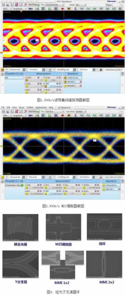
Recently, Yan Jiang, a researcher at the IC Pilot Research and Development Center of the Institute of Microelectronics of the Chinese Academy of Sciences, has made new advances in the development of silicon photonics platforms, completing silicon-based waveguide integrated germanium detectors (Figure 1) and silicon-based modulators (Figure 2). Bleed and get excellent results. Silicon photonics technology is one of the development directions in the post-Moore era of integrated circuits. It aims to develop photonic devices and chips on a silicon-based substrate by using large-scale integrated circuit technology based on CMOS technology, and eventually realizes optoelectronic monolithic integration. The advantages of silicon photonics technology are to make full use of mature CMOS infrastructure and experience, and to achieve mass production at low cost according to market needs. However, there are certain differences between the material selection and process flow of photonic devices and chips and integrated circuits, and the development of related processes is required. In recent years, countries such as Europe and the United States have invested a lot in the field of silicon photonics and accumulated experience, and gradually formed industrial advantages. Although China has achieved remarkable results in the design and production of discrete devices, there is no complete silicon photonics process platform in China. The high-end silicon photonic chips designed in China are basically required to be flowed out of the country, resulting in high cost, long cycle, and difficulty in process customization. Such issues have largely restricted the development of China's silicon photonics technology. The Microelectronics Integrated Circuit Pilot Process R&D Center has a complete 8-inch CMOS process line. Since its completion in 2011, it has successfully completed a number of major national science and technology projects. In 2015, the center combined the development trend of the integration of microelectronics technology and optoelectronics technology, decisively organized the team, and relied on the pilot center CMOS process line to develop silicon photonic process technology. Since the establishment of the Silicon Photonics Team, a large number of meticulous research and development efforts have been carried out. They have also worked closely with the Semiconductor Research Institute of the Chinese Academy of Sciences, the China Electronics 38 Institute, and the Wuhan Institute of Posts and Telecommunications to jointly establish a silicon photonics platform development team. The advantages of each unit have been established and a silicon photonics platform has been established. In the PDK scheme, a library of silicon photon passive and active devices was designed, and multiple process flow experiments were performed. After nearly two years of efforts, a series of silicon photonics flow sheet process modules and a preliminary version of PDK have been successfully developed. The standard cell library mainly includes single-mode waveguides, Y-branches, optical cross-connectors, coupled gratings, and other passive devices, and recently active Successful development of the process will add active devices such as heating electrodes, modulators, and Ge photodetectors to the standard cell library. The success of the active device tapes, together with the silicon photonic passive processes and devices successfully developed by the pilot center in the first half of 2016 (Fig. 3), enables the silicon photonics platform for microelectronics to provide silicon photonics for the industry based on the 180nm process. The capability of tape streaming service has become the first platform to provide users with complete silicon photon MPW and customized tape streaming services based on the 8-inch CMOS process line, which will provide strong support for the research and application development of silicon photonics in China. Trunnion Valve Balls,True Union Ball Valve,Three Way Ball Valve,Ball Valve Shut Off WENZHOU ZHENHONG VALVE BALL CO., LTD , https://www.zhvalveball.com
Progress in development of microelectronics silicon photonics platform